- 您现在的位置:买卖IC网 > Sheet目录317 > C8051T610DB24 (Silicon Laboratories Inc)DAUGHTER BOARD T610 24QFN SOCKET
�� �
�
�C8051T610/1/2/3/4/5/6/7�
�24.2.� SPI0� Master� Mode� Operation�
�A� SPI� master� device� initiates� all� data� transfers� on� a� SPI� bus.� SPI0� is� placed� in� master� mode� by� setting� the�
�Master� Enable� flag� (MSTEN,� SPI0CN.6).� Writing� a� byte� of� data� to� the� SPI0� data� register� (SPI0DAT)� when�
�in� master� mode� writes� to� the� transmit� buffer.� If� the� SPI� shift� register� is� empty,� the� byte� in� the� transmit� buffer�
�is� moved� to� the� shift� register,� and� a� data� transfer� begins.� The� SPI0� master� immediately� shifts� out� the� data�
�serially� on� the� MOSI� line� while� providing� the� serial� clock� on� SCK.� The� SPIF� (SPI0CN.7)� flag� is� set� to� logic�
�1� at� the� end� of� the� transfer.� If� interrupts� are� enabled,� an� interrupt� request� is� generated� when� the� SPIF� flag�
�is� set.� While� the� SPI0� master� transfers� data� to� a� slave� on� the� MOSI� line,� the� addressed� SPI� slave� device�
�simultaneously� transfers� the� contents� of� its� shift� register� to� the� SPI� master� on� the� MISO� line� in� a� full-duplex�
�operation.� Therefore,� the� SPIF� flag� serves� as� both� a� transmit-complete� and� receive-data-ready� flag.� The�
�data� byte� received� from� the� slave� is� transferred� MSB-first� into� the� master's� shift� register.� When� a� byte� is�
�fully� shifted� into� the� register,� it� is� moved� to� the� receive� buffer� where� it� can� be� read� by� the� processor� by�
�reading� SPI0DAT.�
�When� configured� as� a� master,� SPI0� can� operate� in� one� of� three� different� modes:� multi-master� mode,� 3-wire�
�single-master� mode,� and� 4-wire� single-master� mode.� The� default,� multi-master� mode� is� active� when�
�NSSMD1� (SPI0CN.3)� =� 0� and� NSSMD0� (SPI0CN.2)� =� 1.� In� this� mode,� NSS� is� an� input� to� the� device,� and�
�is� used� to� disable� the� master� SPI0� when� another� master� is� accessing� the� bus.� When� NSS� is� pulled� low� in�
�this� mode,� MSTEN� (SPI0CN.6)� and� SPIEN� (SPI0CN.0)� are� set� to� 0� to� disable� the� SPI� master� device,� and�
�a� Mode� Fault� is� generated� (MODF,� SPI0CN.5� =� 1).� Mode� Fault� will� generate� an� interrupt� if� enabled.� SPI0�
�must� be� manually� re-enabled� in� software� under� these� circumstances.� In� multi-master� systems,� devices� will�
�typically� default� to� being� slave� devices� while� they� are� not� acting� as� the� system� master� device.� In� multi-mas-�
�ter� mode,� slave� devices� can� be� addressed� individually� (if� needed)� using� general-purpose� I/O� pins.�
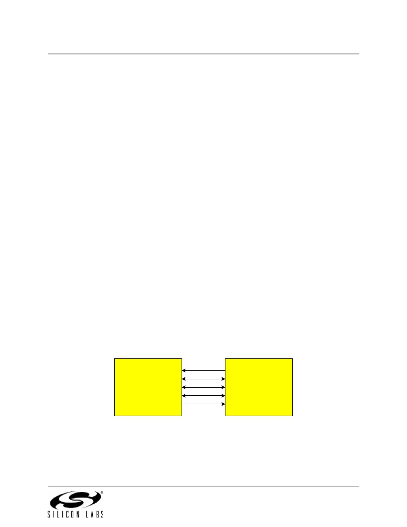
�Figure� 24.2� shows� a� connection� diagram� between� two� master� devices� in� multiple-master� mode.�
�3-wire� single-master� mode� is� active� when� NSSMD1� (SPI0CN.3)� =� 0� and� NSSMD0� (SPI0CN.2)� =� 0.� In� this�
�mode,� NSS� is� not� used,� and� is� not� mapped� to� an� external� port� pin� through� the� crossbar.� Any� slave� devices�
�that� must� be� addressed� in� this� mode� should� be� selected� using� general-purpose� I/O� pins.� Figure� 24.3�
�shows� a� connection� diagram� between� a� master� device� in� 3-wire� master� mode� and� a� slave� device.�
�4-wire� single-master� mode� is� active� when� NSSMD1� (SPI0CN.3)� =� 1.� In� this� mode,� NSS� is� configured� as� an�
�output� pin,� and� can� be� used� as� a� slave-select� signal� for� a� single� SPI� device.� In� this� mode,� the� output� value�
�of� NSS� is� controlled� (in� software)� with� the� bit� NSSMD0� (SPI0CN.2).� Additional� slave� devices� can� be�
�addressed� using� general-purpose� I/O� pins.� Figure� 24.4� shows� a� connection� diagram� for� a� master� device� in�
�4-wire� master� mode� and� two� slave� devices.�
�NSS�
�GPIO�
�Master�
�Device� 1�
�MISO�
�MOSI�
�SCK�
�GPIO�
�MISO�
�MOSI�
�SCK�
�NSS�
�Master�
�Device� 2�
�Figure� 24.2.� Multiple-Master� Mode� Connection� Diagram�
�Rev� 1.1�
�159�
�发布紧急采购,3分钟左右您将得到回复。
相关PDF资料
C8051T630DB20
BOARD SOCKET DAUGHTER 20-QFN
CAN-100
BOARD EVAL RS232 100QFP
CANADAPT28
KIT ADAPTER CANDEMOBOARD 28PLCC
CAT24AA01WI-GT3
IC EEPROM SERIAL 1KB I2C 8SOIC
CAT24AA02WI-G
IC EEPROM SERIAL 2KB I2C 8SOIC
CAT24C01ZI-G
IC EEPROM SERIAL 1KB I2C 8MSOP
CAT24C03WI-G
IC EEPROM SERIAL 2KB I2C 8SOIC
CAT24C04ZI-G
IC EEPROM SERIAL 4KB I2C 8MSOP
相关代理商/技术参数
C8051T610DB28
功能描述:子卡和OEM板 C8051T610 Family Socket Daughtr Board RoHS:否 制造商:BeagleBoard by CircuitCo 产品:BeagleBone LCD4 Boards 用于:BeagleBone - BB-Bone - Open Source Development Kit
C8051T610DB32
功能描述:子卡和OEM板 C8051T610 Family Socket Daughtr Board RoHS:否 制造商:BeagleBoard by CircuitCo 产品:BeagleBone LCD4 Boards 用于:BeagleBone - BB-Bone - Open Source Development Kit
C8051T610DK
功能描述:开发板和工具包 - 8051 C8051T610 Series Development Kit RoHS:否 制造商:Silicon Labs 产品:Development Kits 工具用于评估:C8051F960, Si7005 核心: 接口类型:USB 工作电源电压:
C8051T610-GQ
功能描述:8位微控制器 -MCU 16KB 10ADC 32Pin MCU RoHS:否 制造商:Silicon Labs 核心:8051 处理器系列:C8051F39x 数据总线宽度:8 bit 最大时钟频率:50 MHz 程序存储器大小:16 KB 数据 RAM 大小:1 KB 片上 ADC:Yes 工作电源电压:1.8 V to 3.6 V 工作温度范围:- 40 C to + 105 C 封装 / 箱体:QFN-20 安装风格:SMD/SMT
C8051T610-GQR
功能描述:8位微控制器 -MCU 16KB 10ADC 32Pin MCU RoHS:否 制造商:Silicon Labs 核心:8051 处理器系列:C8051F39x 数据总线宽度:8 bit 最大时钟频率:50 MHz 程序存储器大小:16 KB 数据 RAM 大小:1 KB 片上 ADC:Yes 工作电源电压:1.8 V to 3.6 V 工作温度范围:- 40 C to + 105 C 封装 / 箱体:QFN-20 安装风格:SMD/SMT
C8051T611-GM
功能描述:8位微控制器 -MCU 16KB 10ADC 28Pin MCU RoHS:否 制造商:Silicon Labs 核心:8051 处理器系列:C8051F39x 数据总线宽度:8 bit 最大时钟频率:50 MHz 程序存储器大小:16 KB 数据 RAM 大小:1 KB 片上 ADC:Yes 工作电源电压:1.8 V to 3.6 V 工作温度范围:- 40 C to + 105 C 封装 / 箱体:QFN-20 安装风格:SMD/SMT
C8051T611-GMR
功能描述:8位微控制器 -MCU 16KB 10ADC 28Pin MCU RoHS:否 制造商:Silicon Labs 核心:8051 处理器系列:C8051F39x 数据总线宽度:8 bit 最大时钟频率:50 MHz 程序存储器大小:16 KB 数据 RAM 大小:1 KB 片上 ADC:Yes 工作电源电压:1.8 V to 3.6 V 工作温度范围:- 40 C to + 105 C 封装 / 箱体:QFN-20 安装风格:SMD/SMT
C8051T612-GQ
功能描述:8位微控制器 -MCU 8KB 10ADC 32Pin MCU RoHS:否 制造商:Silicon Labs 核心:8051 处理器系列:C8051F39x 数据总线宽度:8 bit 最大时钟频率:50 MHz 程序存储器大小:16 KB 数据 RAM 大小:1 KB 片上 ADC:Yes 工作电源电压:1.8 V to 3.6 V 工作温度范围:- 40 C to + 105 C 封装 / 箱体:QFN-20 安装风格:SMD/SMT